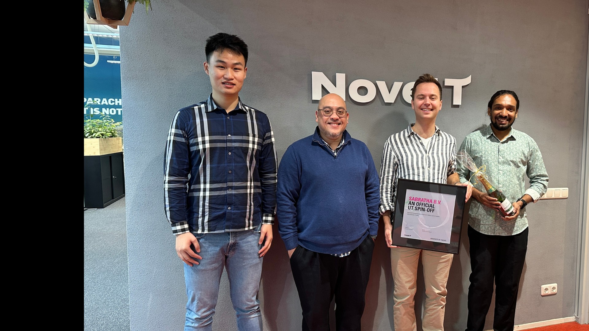
cases >> Sabratha
INTEGRATED PHOTONICS CHIP TECHNOLOGY FOR A WIRELESS AND TELECOMMUNICATION REVOLUTION
INTEGRATED PHOTONICS CHIP TECHNOLOGY FOR A WIRELESS AND TELECOMMUNICATION REVOLUTION
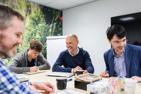
Wireless communication has become commonplace over the past few decades. However, each next generation of wireless technology comes with its own challenges. How can we connect more devices on a network that’s ten times faster without renewing our physical infrastructure every other year? With their thin-film lithium niobate (TFLN) photonic chip, the team of UT spin-off Sabratha has the answer. CEO Kees Franken and CTO Steven Ye talk about their technology and their spin-off journey.
Every day, we generate more and more data. In 2015, it was estimated that we generated 15.5 zettabytes (15.5 billion terabytes) of data in that year, globally. Ten years later, in 2025, we’re at a whopping 181 zettabytes - over 11 times more. “Our technology has to keep up with that growth,” Kees explains. “And a good example lies in wireless communications, where traditional technology that’s used for 4G and 5G probably won’t suffice for 6G. The Internet of Things (IoT) is also coming, and we need a reliable network for that. In particular, we see an opportunity with the structure that’s connecting all the wireless base stations: the optical fiber network. Recent years have proven that it’s a major challenge to lay down fiber networks as is, and it’s not feasible to keep putting extra fibers down, especially in urban areas or transatlantic. That’s why, with our chip, we want to put as much data into a single fiber as possible, while processing more data in the optical domain as well. We want to revolutionize the next-gen wireless communication markets with our chips.”
Interaction between light and sound
That is what the Sabratha team has been working on for decades. The team created a photonic chip with a new material: thin-film lithium niobate. Steven: “It allows you to transfer data at really high speeds - much faster and more energy efficient than with current photonic technologies. More importantly, our company’s uniqueness is that we exploit the Stimulated Brillouin Scattering effect, where light interacts with acoustic waves.” With this, their chip can optically process data using crucial filtering functionalities. “The research group we spun out of was the first to measure this Brillouin effect in this chip platform. That was the most important discovery from my PhD, and it got published in a high-impact journal (Science Advances). This unique filtering and processing capability makes us the only ones doing this commercially, which gives us a distinctive position in the market.”
From research to synergetic collaboration
The innovation took years of research, led by renowned professor David Marpaung. While Steven did his PhD in this research group at the UT, Kees did 2 years of his PhD at Harvard University in the research group that developed the TFLN material. “I learned how to make those chips there,” says Kees. “Simultaneously, the group in Twente was building up the chip technology here. That’s why we saw potential to team up: Steven is the expert in stimulated Brillouin scattering, and my expertise is in the making of these chips.” Steven adds: “And then we have Akshay Keloth, who developed the cleanroom process here from the ground up. He spent almost a whole year trying to bring the material to the Netherlands, into the cleanroom. All that expertise added up makes for a very synergetic collaboration to further improve the performance of our chip.”
Entrepreneurial university
To get to where they are now, they got some help along the way. Steven: “The cleanroom staff at MESA+ was very helpful in making this all happen. You see, it’s rather daunting for a cleanroom to introduce a new material because it has all kinds of requirements to avoid contamination. They were really collaborative.” Kees adds: “That’s really what makes the UT an entrepreneurial university. There’s also a plethora of support from Novel-T for researchers wanting to spin out. The founding process went really fast, and the dealmaking with the university was done very respectfully for both sides. The knowledge transfer infrastructure is very mature and complete. Furthermore, there is a whole community of ChipTech startups here in Twente that we work with and learn from, like Quix Quantum and QSA Technology. Everyone just really wants to help each other. It’s ‘noaberschap’ (neighborliness, ed.) in a high-tech jacket.”
Going down in history
The company has a good reason to stay in Twente for the foreseeable future. Steven: “Currently, we still share an office with PhD students, so having our own office would be nice to start with. But we have high ambitions, meaning that we want to grow into the global market. We want to serve not only Europe, but also Asia and maybe even the rest of the world. The chip foundry of New Origin would be great for that, especially if we want to realize our dream: to become the next Nvidia. It started as a joke by David, but now that’s truly what we work towards.” Their ambitions echo through in their name: Sabratha comes from the ancient city in Libya. More specifically, from its amphitheater, where The Beatles were supposed to give their final concert (David is a huge fan). That concert never happened, but it didn’t make Sabratha less immortal. Kees: “We want to build something that lasts.”

"We want to revolutionize the next-gen 6G wireless communication market with our chips."
Kees Franken
CEO SabrathaMore about
Sabratha
Sabratha Photonics is a 2025 deep-tech startup dedicated to commercializing over five years of IP and know-how in TFLN technology, developed at a leading European photonics laboratory, the University of Twente in the Netherlands.